If you want optical coatings to do their job, you have to get the film thickness and refractive indices right—being off by just a few nanometers changes the interference pattern completely. This Thin Film Optics Calculator lets you work out reflectance, transmittance, phase shifts, and whether you’ll get constructive or destructive interference. You punch in your indices, thickness, wavelength, and incident angle. This isn’t just for lab optics: you’ll run into these principles in photonics, semiconductors, and anywhere else optical coatings need to hit a specific spectrum before you ever run the deposition tool. Down below you’ll find the basic equations, a worked multi-wavelength example, background on Fresnel coefficients and quarter-wave stacks, plus an FAQ with details that’ve come up in real engineering problems.
What is thin film optics?
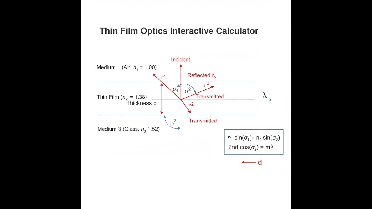
Thin film optics is about how light interacts with a transparent layer only tens to hundreds of nanometers thick. The main thing: light reflects from both top and bottom surfaces. These two beams travel slightly different distances and interfere—depending on thickness and wavelength, you’ll either amplify or cancel the reflected light.
Simple Explanation
Think of it like dropping two pebbles in water: waves can line up (constructive) or flatten each other out (destructive). That’s what happens with light in a thin film. The top and bottom reflections combine—sometimes you get a boost, sometimes a drop, depending on the path length difference. That’s all the color you see in soap bubbles, or the colored coatings on camera lenses—it’s interference, not pigment.
📐 Browse all 1000+ Interactive Calculators
Thin Film Interference Diagram

How to Use This Calculator
- Select a calculation mode from the dropdown — options include Reflectance & Phase Shift, Interference Condition, Required Film Thickness, Wavelength from Interference, Anti-Reflective Coating Design, and Quarter-Wave Stack Analysis.
- Enter the refractive indices for the incident medium (n₁), film (n₂), and substrate (n₃) as applicable, along with film thickness in nm, wavelength in nm, and incident angle in degrees.
- Check that all inputs are physically valid — refractive indices must be greater than zero, angle must be between 0° and 90°, and high-index value must exceed low-index value for quarter-wave stack mode.
- Click Calculate to see your result.
Interactive Thin Film Optics Calculator
This calculator is intended for education, concept evaluation, and preliminary design. Results are based on the equations and assumptions described on this page, but cannot account for every real-world load case, tolerance, material property, environmental condition, installation detail, safety factor, code, or regulatory requirement. Verify all inputs, assumptions, units, and results independently before selecting components or using the result in a real application. Safety-critical, structural, medical, lifting, transportation, or regulated applications must be reviewed by a qualified engineer.
Thin Film Optics Interactive Visualizer
Watch how light waves interfere as they reflect from top and bottom surfaces of a thin film coating. Adjust film thickness and wavelength to see constructive or destructive interference in real-time.
REFLECTANCE
1.3%
PHASE SHIFT
180°
CONDITION
MIN
FIRGELLI Automations — Interactive Engineering Calculators
Governing Equations
Here are the key equations for thin film optics. Snell’s Law will get you the angle in the film and substrate based on your input values. Check units—the calculators handle nm and degrees.
Snell's Law at Film Interfaces
n1 sin θ1 = n2 sin θ2 = n3 sin θ3
where:
- n1, n2, n3 = refractive indices of incident medium, film, and substrate (dimensionless)
- θ1, θ2, θ3 = angles of incidence, refraction in film, and transmission (radians or degrees)
The following equation gives the phase shift as light passes through the film. This is the path difference—what sets up the interference pattern between the two reflected beams.
Optical Path Difference
δ = (4π n2 d cos θ2) / λ
where:
- δ = phase shift between rays reflected from top and bottom surfaces (radians)
- d = physical thickness of film (nm or m)
- λ = wavelength of light in vacuum (nm or m)
Below is how you calculate the amplitude reflection coefficients for each interface—these matter for calculating net reflectance, especially if you’re choosing layer materials.
Fresnel Reflection Coefficients
r12 = (n1 cos θ1 − n2 cos θ2) / (n1 cos θ1 + n2 cos θ2)
r23 = (n2 cos θ2 − n3 cos θ3) / (n2 cos θ2 + n3 cos θ3)
where:
- r12 = amplitude reflection coefficient at air-film interface (dimensionless, −1 to +1)
- r23 = amplitude reflection coefficient at film-substrate interface (dimensionless, −1 to +1)
This equation rolls up everything above to get the net reflectance, combining both interfaces with interference included. It’s dead-on for non-absorbing films. If your application involves absorption, this will be an overestimate.
Net Reflectance
R = (r122 + r232 + 2r12r23 cos δ) / (1 + r122r232 + 2r12r23 cos δ)
where:
- R = intensity reflectance (dimensionless, 0 to 1, often expressed as percentage)
- Transmittance T = 1 − R (assuming negligible absorption)
Here’s the standard equation for working out the film thickness needed for either constructive or destructive interference, based on your design wavelength. Useful for AR coatings and filter design.
Constructive and Destructive Interference Conditions
Constructive (maximum reflection): 2n2 d cos θ2 = m λ
Destructive (minimum reflection): 2n2 d cos θ2 = (m + ½) λ
where:
- m = interference order (integer: 0, 1, 2, 3...)
- Conditions assume one interface has a phase change of π upon reflection
If you want a quarter-wave single-layer AR coating, these formulas give you the ideal refractive index and thickness. This is as good as it gets for a single layer at one wavelength—multilayers are needed for broadband.
Quarter-Wave Anti-Reflective Coating
n2 = —√(n1 n3)
d = λ / (4n2)
where:
- Optical thickness = n2 d = λ/4 (quarter-wave condition)
- Perfect cancellation occurs when n2 is geometric mean of surrounding indices
Simple Example
Example: you’ve got a MgF₂ film (n₂ = 1.38) on glass (n₃ = 1.52), light comes in at 550 nm (green) at normal incidence, thickness d = 100 nm.
- Optical thickness = 1.38 × 100 = 138 nm
- Phase shift δ = (4π × 138) / 550 = 3.15 rad (about 180°) — close to the quarter-wave minimum condition
- Result: Reflectance R ≈ 1.3%. For comparison, uncoated glass would reflect about 4.3% under the same conditions.
Theory & Practical Applications
Physical Mechanism of Thin Film Interference
Thin film interference is just the result of light bouncing between two surfaces so close together that their reflected waves overlap and interact. As light hits a thin transparent film, some of it bounces off the top, some makes it through and bounces off the bottom, and the two reflected beams exit at the same angle. If the film’s thickness and wavelength line up just right, those beams can add or cancel. This only works well if the film thickness is close to the wavelength of the light, and if the light is reasonably coherent—otherwise, the effect washes out.
One nuance that trips up a lot of people: the reflected wave often picks up a 180° phase shift when bouncing off a material with higher refractive index. In a basic air–film–glass stack, both the air–film and film–glass reflections may flip phase. It’s the relative phase between the two returned beams that matters—a detail that changes which thicknesses give you minima and maxima. You’ll notice for thin films the formula for maximum reflectance looks almost backwards compared to double-slit: it’s because you might have phase shifts at both boundaries, so the internal path length alone sets the result.
Fresnel Coefficients and Reflectance Engineering
The amplitude coefficients r₁₂ and r₂₃ tell you how much of the light gets reflected at each interface. For normal incidence (simple case), r₁₂ = (n₁ − n₂)/(n₁ + n₂), and r₂₃ = (n₂ − n₃)/(n₂ + n₃). Negative values mean the wave flips phase; positive, no flip. At off-normal angles, you have to split into s- and p-polarizations, and things get interesting at the Brewster angle: p-polarized reflection drops to zero, which is why you sometimes see polarizing windows at that angle to skip coatings altogether.
Plugging these into the full reflectance formula shows you’ll get oscillations in reflectance versus wavelength or thickness—the crux of interference. For a real-world MgF₂-on-glass film of 100 nm, scanning the wavelength from blue to red gives those transmission “fringes,” with a neat dip near 550 nm. In a broader context, actual material indices aren’t constant with wavelength (dispersion), so your “perfect” minimum might shift or broaden in a real application. If you need low reflectance across a wide band, you’ll need stacks of alternating high/low-index layers, and, realistically, a computer to optimize them for your band and angles.
Industrial Applications Across Photonics and Manufacturing
AR coatings are just about everywhere—from eyeglasses and camera lenses to solar panels and displays. A single MgF₂ layer can bring reflectance down from 4.3% to about 1.3% at the target wavelength. If the project wants broadband performance, you’ll layer up (SiO₂, Al₂O₃, Ta₂O₅, TiO₂, etc): get the reflectance well below 1% at most of the spectrum, which stacks up (literally) if you have a multi-element lens assembly.
Semiconductor fabs lean on thin film interference for monitoring during film growth—shine a probe, watch the oscillations, and you can resolve thickness changes to the angstrom in real time. This is routine with SiO₂ or Si₃N₄ on silicon for process control in making transistors or dielectrics. You’ll see similar approaches with III–V semiconductors, where exact layer control is crucial for things like laser diodes.
For wavelength-selective filters and mirrors, you use multilayered quarter-wave stacks—alternating high and low index films, each λ/4 thick for the design wavelength. This gives sharp bandpass or blocking outside that band. For example, mirrors for red HeNe lasers (632.8 nm) often use TiO₂ and SiO₂ multilayers. Reflectance increases quickly with more pairs, but physical limitations (absorption, stress, etc) keep this from continuing forever.
Design Considerations and Practical Limitations
If temperature changes, so does the refractive index and the interference pattern, shifting your reflection minimum. Coefficient values are usually low, but if the device swings tens of degrees, the coating’s performance can move a few nanometers in wavelength, which may or may not matter for your application. Sometimes you balance this by athermal design or temperature control.
Thick films and many-layer stacks can stress the substrate, leading to warping, delamination, or even cracks—especially if you haven’t balanced tensile/compressive layers. Sputtered SiO₂, for example, is very tensile; TiO₂ is compressive. Stack enough, and you can compensate, but there’s a practical thickness ceiling, usually under 10 μm total, especially on glass. Extra process tricks like plasma pretreatment or ion-assisted deposition are common when you need better adhesion or lower overall film stress.
Most materials are flagged as “transparent” for visible and near-IR, but at certain wavelengths, or with thick multipair mirrors, even low absorption eats a measurable chunk of your incident power. If you’re running high-powered lasers, tiny absorption adds up, causing heating issues, shifting performance, or even leading to catastrophic damage at the highest intensities. Sometimes you’ll pay more for an oxide with less absorption if power handling is critical.
Worked Example: Designing a V-Coat for Dual Wavelengths
Let’s say you need a coating on glass (n₃ = 1.52) to work at two different laser lines: 488 nm (argon-ion) and 632.8 nm (HeNe). A single-layer can’t hit both, so you go with a two-layer (V-coat) design.
Step 1: Choose materials. MgF₂ (n₁ = 1.38) on the outside, Al₂O₃ (n₂ = 1.63) beneath. Pick for index spacing, chemical stability, and what works in your deposition tool.
Step 2: Structure. Air | MgF₂ (d₁) | Al₂O₃ (d₂) | Glass. The job is to find d₁ and d₂ for low reflectance at both lines.
Step 3: Start with quarter-waves at the geometric mean wavelength λ_avg = √(488 × 632.8) ≈ 555.5 nm; so d₁ = 555.5 / (4 × 1.38) ≈ 100.6 nm, d₂ = 555.5 / (4 × 1.63) ≈ 85.2 nm.
Step 4: Reflectance at 488 nm. Calculate phase for each layer. For MgF₂, δ₁ = (4π × 1.38 × 100.6)/488 = 1.129 rad; for Al₂O₃, δ₂ = (4π × 1.63 × 85.2)/488 = 1.433 rad. Use matrix methods to get total reflectance—here, about 2.3% at 488 nm.
Step 5: Reflectance at 632.8 nm. Phase terms: δ₁ = (4π × 1.38 × 100.6)/632.8 = 0.871 rad; δ₂ = (4π × 1.63 × 85.2)/632.8 = 1.105 rad. Reflectance comes out to about 1.9% at 632.8 nm.
Step 6: Refine thickness. To get both values lower, run an optimization (even a spreadsheet works for a two-layer stack). You end up, after tweaking, with d₁ ≈ 98.3 nm and d₂ ≈ 89.7 nm, getting reflectance down to 0.8% at 488 nm and 0.6% at 632.8 nm. That’s what you can expect from a properly tuned V-coat. If you’re building a production run, let tolerances guide you—manufacturers typically control thickness to ±2 nm, so plan for a little extra margin.
Step 7: Thickness tolerance. Monte Carlo or simple min/max sweeps show how much your reflectance rises as layer thicknesses drift with process error. For this design, the variation from ±2 nm is modest: mean reflectance still stays low, but worst-case could creep up to ~2%. Good enough for most practical uses—if you need better, add layers, but deposition gets trickier.
Advanced Topics: Dispersion, Anisotropy, and Nonlinear Effects
Material indices aren’t constants—most vary a little with wavelength (chromatic dispersion). Even for “simple” MgF₂, n ranges from 1.37 to 1.39 across the visible. This means your carefully chosen thickness only lines up with a perfect null at one wavelength; elsewhere, you’ll see drift. Broadband AR designs use more layers and computer optimization to flatten the reflectance across the visible. Modern optical design software can crank out 20+ layer solutions that hit very low reflectance across a wide band.
Birefringent materials (like quartz or calcite) have different indices for different polarizations, so s and p polarizations see different thicknesses—complicates matters, but if you’re building polarizing optics or waveplates, you can actually use this effect. Polarization optics often exploit these differences to reach extreme contrast ratios.
At high light intensities (ultrafast or high-energy lasers), the refractive index can change dynamically with optical power. This shifts your interference conditions and can lead to self-focusing or unwanted spectral changes. When this matters, you’ll see custom coatings (like chirped mirrors) engineered to hit not just a reflectance target but a specific phase response to avoid pulse distortion.
Metrology and Characterization Techniques
To measure the film’s thickness and index, ellipsometry is the go-to method—it measures how the polarization of light changes on reflection to back out both parameters, usually to better than a nanometer. If you want a non-contact, fast check across a surface, white-light interferometry or OCT will do the job—common for QA on AR lenses and for mapping thickness across wafers in a semiconductor fab.
For more calculations like this—on diffraction, polarization, and related optics problems—check the engineering calculator library.
Frequently Asked Questions
Free Engineering Calculators
Explore our complete library of free engineering and physics calculators.
Browse All Calculators →🔗 Explore More Free Engineering Calculators
About the Author
Robbie Dickson — Chief Engineer & Founder, FIRGELLI Automations
Robbie Dickson brings over two decades of engineering expertise to FIRGELLI Automations. With a distinguished career at Rolls-Royce, BMW, and Ford, he has deep expertise in mechanical systems, actuator technology, and precision engineering.
Video Walkthrough - How to Use This Calculator
Need to implement these calculations?
Explore the precision-engineered motion control solutions used by top engineers.


