Designing AC circuits with resistors, inductors, and capacitors means dealing with impedance that changes with frequency — and getting that wrong means filters that don't filter, resonant circuits that don't resonate, and power stages that waste energy as heat. Use this RLC Impedance Interactive Calculator to calculate total impedance, phase angle, resonant frequency, quality factor, power factor, and bandwidth using resistance, inductance, capacitance, and frequency as inputs. It matters across filter design, RF matching networks, and industrial power factor correction — anywhere frequency-dependent circuit behavior determines performance. This page includes the core impedance formulas, a worked example, full theory on series and parallel RLC behavior, and a practical FAQ.
What is RLC impedance?
RLC impedance is the total opposition to AC current flow in a circuit containing a resistor (R), inductor (L), and capacitor (C). Unlike resistance, it changes with frequency — which is what makes RLC circuits useful for filtering, tuning, and power control.
Simple Explanation
Think of it like a pipe system where water flow depends not just on the pipe's narrowness (resistance), but also on a spring (capacitor) and a flywheel (inductor) — both of which push back harder or softer depending on how fast the flow is changing. At one specific frequency, the spring and flywheel effects cancel each other out exactly, and the circuit hits resonance. That's the sweet spot RLC circuit design is usually aiming for.
📐 Browse all 1000+ Interactive Calculators
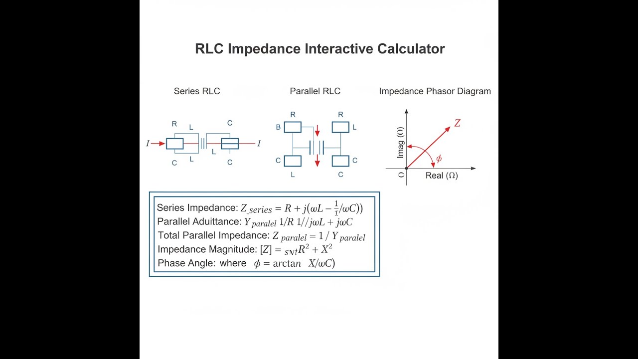
RLC Circuit Diagrams

RLC Impedance Calculator
How to Use This Calculator
- Select a calculation mode from the dropdown — Series RLC, Parallel RLC, Resonant Frequency, Quality Factor, Power Factor, or Bandwidth.
- Enter your component values: Resistance in ohms (Ω), Inductance in millihenries (mH), and Capacitance in microfarads (μF).
- Enter the operating frequency in hertz (Hz) — leave this blank if you selected Resonant Frequency mode.
- Click Calculate to see your result.
RLC Impedance Interactive Visualizer
Explore how resistance, inductance, and capacitance combine to create frequency-dependent impedance in AC circuits. Watch impedance magnitude and phase angle change dramatically as you approach resonance frequency.
IMPEDANCE |Z|
100 Ω
PHASE ANGLE
0°
RESONANCE
1006 Hz
FIRGELLI Automations — Interactive Engineering Calculators
RLC Impedance Equations
Use the formula below to calculate reactance components for inductors and capacitors.
Reactance Components
XL = ωL = 2πfL
XC = 1/(ωC) = 1/(2πfC)
XL = Inductive reactance (Ω)
XC = Capacitive reactance (Ω)
ω = Angular frequency (rad/s)
f = Frequency (Hz)
L = Inductance (H)
C = Capacitance (F)
Use the formula below to calculate series RLC impedance magnitude and phase angle.
Series RLC Impedance
Z = R + j(XL - XC)
|Z| = √(R² + (XL - XC)²)
φ = arctan((XL - XC)/R)
Z = Complex impedance (Ω)
R = Resistance (Ω)
φ = Phase angle (degrees or radians)
j = Imaginary unit (√-1)
Use the formula below to calculate parallel RLC admittance and equivalent impedance.
Parallel RLC Admittance
Y = 1/R + j(1/XC - 1/XL)
|Y| = √((1/R)² + (1/XC - 1/XL)²)
Z = 1/Y
Y = Complex admittance (S)
G = 1/R = Conductance (S)
B = 1/XC - 1/XL = Susceptance (S)
Use the formula below to calculate resonant frequency and quality factor.
Resonance & Quality Factor
f0 = 1/(2π√(LC))
Qseries = ω0L/R = 1/(ω0RC)
BW = f0/Q
f0 = Resonant frequency (Hz)
Q = Quality factor (dimensionless)
BW = Bandwidth at half-power points (Hz)
Simple Example
Series RLC circuit at 1000 Hz with R = 100 Ω, L = 10 mH, C = 2.533 μF:
- Inductive reactance XL = 2π × 1000 × 0.01 = 62.83 Ω
- Capacitive reactance XC = 1 / (2π × 1000 × 0.000002533) = 62.83 Ω
- Net reactance X = 62.83 − 62.83 = 0 Ω (resonance)
- Total impedance |Z| = √(100² + 0²) = 100 Ω, phase angle = 0°
Theory & Practical Applications of RLC Impedance
RLC impedance represents the frequency-dependent opposition to alternating current flow in circuits containing resistance, inductance, and capacitance. Unlike purely resistive circuits where opposition remains constant, RLC impedance varies with frequency due to the reactive energy storage in inductors and capacitors. This frequency dependence enables critical applications in filtering, resonance, impedance matching, and power factor correction across electronics, power systems, and RF design. Understanding RLC impedance behavior requires analyzing both magnitude and phase relationships between voltage and current through complex phasor mathematics.
Series vs. Parallel RLC Configuration Behavior
Series RLC circuits exhibit impedance minima at resonance, where inductive and capacitive reactances cancel precisely. At resonance (f0 = 1/(2π√LC)), impedance equals pure resistance R, and current reaches maximum for a given voltage. Below resonance, capacitive reactance dominates (XC greater than XL), creating a capacitive circuit with leading current. Above resonance, inductive reactance dominates, producing lagging current. This behavior makes series RLC circuits ideal for bandpass filtering in radio receivers and signal processing applications where maximum current flow at a specific frequency is desired.
Parallel RLC circuits demonstrate opposite behavior: impedance reaches a maximum at resonance rather than a minimum. The parallel resonant impedance equals R(L/C)/R = L/(RC) for ideal components, often orders of magnitude higher than the branch resistances. This impedance peak creates the "tank circuit" behavior fundamental to LC oscillators, where energy oscillates between magnetic field storage in the inductor and electric field storage in the capacitor. Parallel resonant circuits find extensive use in RF power amplifiers, where high impedance at the operating frequency maximizes voltage gain while presenting low impedance to harmonics for filtering.
Quality Factor and Bandwidth Relationships
Quality factor Q quantifies the ratio of energy stored to energy dissipated per cycle in resonant circuits. For series configurations, Q = ω0L/R = 1/(ω0RC) = (1/R)√(L/C), representing the voltage magnification at resonance. High-Q circuits (Q greater than 10) exhibit sharp resonance peaks with narrow bandwidths, essential for selective filtering in communication receivers where adjacent channel rejection demands selectivity factors exceeding 100. The bandwidth BW = f0/Q defines the frequency range between half-power points where circuit response drops to 70.7% of maximum. A practical AM radio IF filter at 455 kHz with Q = 50 provides bandwidth BW = 9.1 kHz, sufficient for 5 kHz audio bandwidth while rejecting adjacent 10 kHz channels.
However, Q-factor limitations emerge in practical circuits. Inductor equivalent series resistance (ESR) from wire resistance and core losses, capacitor ESR from dielectric losses, and skin effect at high frequencies all reduce achievable Q. Real-world RF inductors rarely exceed Q = 200 at VHF frequencies, limiting filter selectivity. This non-ideality necessitates multi-stage filter designs where cascaded lower-Q stages achieve overall selectivity that single-stage circuits cannot provide. Furthermore, high-Q circuits exhibit increased sensitivity to component tolerances: a 5% capacitance variation in a Q = 100 circuit shifts resonant frequency by approximately 2.5%, potentially moving the passband entirely off the desired frequency in precision applications.
Impedance Transformation and Matching Networks
RLC networks enable impedance transformation essential for maximum power transfer between sources and loads with different impedances. The L-match network, consisting of series and shunt reactive elements, can transform any resistance to any other resistance at a specific frequency while simultaneously providing reactive compensation. For example, matching a 50Ω source to a 200Ω antenna load at 100 MHz requires calculating series reactance Xs = √(RL(RL - Rs)) = √(200(200-50)) = 173.2Ω and shunt reactance Xp = RL√(Rs/(RL - Rs)) = 200√(50/150) = 115.5Ω. These reactances translate to specific component values: Cseries = 9.2 pF and Lshunt = 184 nH for this transformation.
T-match and pi-match networks extend this concept to provide adjustable impedance transformation ratios with multiple frequency responses. Pi-networks, common in RF power amplifiers, use capacitive input and output with series inductance to match low transistor output impedance (typically 2-10Ω) to standard 50Ω loads while simultaneously providing harmonic filtering. The loaded Q of the matching network (typically 3-10 in broadband applications) determines both bandwidth and harmonic attenuation: Q = 5 provides approximately 14 dB second harmonic suppression, while Q = 10 achieves 20 dB suppression but reduces bandwidth by a factor of two.
Power Factor Correction in AC Systems
Industrial three-phase power systems commonly exhibit power factors of 0.7-0.85 lagging due to inductive loads from motors, transformers, and fluorescent lighting. This lagging current increases I²R losses in distribution wiring and reduces system capacity without delivering additional real power. Power factor correction capacitors, sized to supply the reactive power demanded by inductive loads, bring power factor toward unity. For a 100 kW induction motor operating at 0.8 power factor (φ = 36.87°), reactive power Q = P tan(φ) = 100 × 0.75 = 75 kVAR. Installing 75 kVAR of capacitance (approximately 135 μF per phase at 480V, 60 Hz) raises power factor to near unity, reducing line current from 150A to 120A and decreasing distribution losses by 36%.
However, overcorrection creates leading power factor, potentially causing resonance with system inductance and voltage instability. Switched capacitor banks with automatic controllers monitor power factor continuously and engage capacitor stages in 10-25 kVAR increments to maintain power factor between 0.95 and 1.0. Harmonic considerations further complicate modern correction systems: variable frequency drives and switching power supplies inject harmonic currents that can resonate with correction capacitors, creating voltage distortion and equipment damage. Detuned capacitor banks, incorporating series reactors tuned below the 5th harmonic (250 Hz at 60 Hz fundamental), prevent harmonic resonance while maintaining fundamental frequency correction.
Practical Worked Example: Designing a 10.7 MHz IF Filter
Design a series RLC bandpass filter for an FM receiver intermediate frequency stage with the following specifications:
- Center frequency: f0 = 10.7 MHz
- Bandwidth: BW = 200 kHz (for 150 kHz FM signal plus guardband)
- Source and load impedance: 50Ω
- Available inductor: L = 1 μH with QL = 80
Step 1: Calculate required capacitance for resonance
From f0 = 1/(2π√LC), rearranging for C:
C = 1/(4π²f₀²L) = 1/(4π² × (10.7×10⁶)² × 1×10⁻⁶) = 220.3 pF
Step 2: Determine inductor equivalent series resistance
At resonance, XL = 2πf0L = 2π × 10.7×10⁶ × 1×10⁻⁶ = 67.23Ω
QL = XL/RL, therefore RL = XL/QL = 67.23/80 = 0.840Ω
Step 3: Calculate required loaded Q for specified bandwidth
Qloaded = f0/BW = 10.7×10⁶/200×10³ = 53.5
Step 4: Determine additional resistance needed for bandwidth
Qloaded = XL/Rtotal, so Rtotal = XL/Qloaded = 67.23/53.5 = 1.257Ω
Required external resistance: Rext = Rtotal - RL = 1.257 - 0.840 = 0.417Ω
Step 5: Design impedance matching network
The resonant circuit impedance (1.257Ω) must be transformed to 50Ω for proper system matching. Using a tapped inductor approach with tap position n = √(Rload/Rresonant) = √(50/1.257) = 6.31. This requires tapping the inductor at 1/6.31 = 15.8% from the grounded end. Alternatively, a capacitive voltage divider with C1 = 1.39 nF and C2 = 220 pF provides the transformation, where C2 is the resonant capacitor.
Step 6: Verify insertion loss and selectivity
At resonance with proper matching, insertion loss ≈ 0.5 dB (primarily from inductor Q). At ±100 kHz offset (band edges), response drops to -3 dB by design. At ±300 kHz (adjacent channel), response is:
Attenuation = 20 log₁₀(1 + Q²((f/f₀) - (f₀/f))²)^0.5 = 20 log₁₀(1 + 53.5²×(0.056)²)^0.5 = 20.1 dB
This provides adequate adjacent channel rejection for FM broadcast applications. The final design uses L = 1 μH (tapped at 16% for matching), C = 220 pF, with total circuit Q = 53.5 achieving 200 kHz bandwidth centered at 10.7 MHz.
Skin Effect and High-Frequency Impedance Behavior
At frequencies above 1 MHz, skin effect concentrates current near conductor surfaces, increasing effective resistance. Skin depth δ = √(2ρ/(ωμ)) decreases with frequency: for copper at 10 MHz, δ = 21 μm, while at 1 GHz, δ = 2.1 μm. A 1 mm diameter wire exhibits DC resistance of 21.5 mΩ/m, but at 10 MHz, AC resistance increases to approximately 0.34 Ω/m — a 16-fold increase. This dramatically reduces inductor Q at RF frequencies, necessitating litz wire (individually insulated strands) for HF applications or hollow tube conductors for VHF/UHF.
Parasitic capacitance between inductor turns and between component leads creates unintended resonances at high frequencies. A typical through-hole ceramic capacitor exhibits 2-3 nH lead inductance, creating self-resonance at frequencies where XL = XC. A 100 nF capacitor with 3 nH lead inductance resonates near 9 MHz, above which it behaves inductively rather than capacitively. Surface-mount components reduce parasitic inductance to 0.5-1 nH, extending useful frequency range into VHF. Professional RF design requires full S-parameter characterization of components across the operating frequency range, as simple RLC models fail to predict impedance behavior beyond the first resonance.
For comprehensive guidance on AC circuit analysis and impedance calculations, explore the full collection at our engineering calculator library.
Frequently Asked Questions
▼ Why does impedance in series RLC circuits reach minimum at resonance while parallel circuits reach maximum?
▼ How do component tolerances affect RLC circuit resonant frequency and bandwidth in practical applications?
▼ What causes the power factor to differ from unity in RLC circuits, and why does this matter for power systems?
▼ How does skin effect limit inductor Q at high frequencies, and what design techniques compensate for this limitation?
▼ Why do impedance matching networks often use reactive elements exclusively, and when must resistive elements be included?
▼ What physical mechanisms limit the maximum achievable Q in practical LC resonators, and how do engineers work around these limits?
Free Engineering Calculators
Explore our complete library of free engineering and physics calculators.
Browse All Calculators →— - Explore More Free Engineering Calculators
- Resistor Color Code Calculator
- Capacitor Charge Discharge Calculator — RC Circuit
- RLC Circuit Calculator — Resonance Impedance
- Low-Pass RC Filter Calculator — Cutoff Frequency
- Cutoff Frequency Calculator
- Inductor Energy Calculator
- Capacitor Energy Calculator
- Power Factor Calculator and Correction
- Wire Gauge Calculator — Voltage Drop AWG
- Voltage Divider Calculator — Output Voltage from Two Resistors
About the Author
Robbie Dickson — Chief Engineer & Founder, FIRGELLI Automations
Robbie Dickson brings over two decades of engineering expertise to FIRGELLI Automations. With a distinguished career at Rolls-Royce, BMW, and Ford, he has deep expertise in mechanical systems, actuator technology, and precision engineering.
Need to implement these calculations?
Explore the precision-engineered motion control solutions used by top engineers.


