Designing optical coatings means controlling exactly how much light reflects or transmits at each interface — and getting it wrong by even a few nanometers of film thickness changes your interference condition entirely. Use this Thin Film Optics Interactive Calculator to calculate reflectance, transmittance, phase shifts, and constructive or destructive interference conditions using refractive indices, film thickness, wavelength, and angle of incidence. It matters in photonics, semiconductor process monitoring, and precision optics — anywhere a coating's spectral performance needs to be predictable before you deposit a single layer. This page includes the governing equations, a worked multi-wavelength design example, full theory on Fresnel coefficients and quarter-wave stacks, and a detailed FAQ.
What is thin film optics?
Thin film optics describes how light behaves when it passes through or reflects off a very thin transparent layer — typically just tens to hundreds of nanometers thick. The reflected beams from the top and bottom surfaces of the film interfere with each other, either amplifying or canceling the reflected light depending on the film thickness and wavelength.
Simple Explanation
Think of it like ripples on water — when 2 waves meet, they either add together (constructive) or cancel out (destructive). A thin film does the same thing with light: the beam reflecting off the top surface and the beam reflecting off the bottom surface travel slightly different distances, so they can reinforce or cancel each other. That's why soap bubbles show colors and why camera lenses have that faint purple or green tint — both are thin film interference in action.
📐 Browse all 1000+ Interactive Calculators
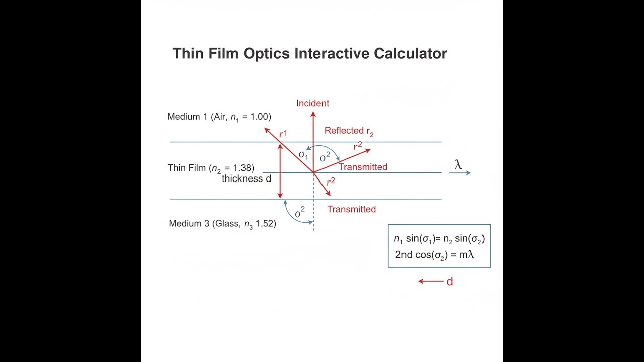
Thin Film Interference Diagram

How to Use This Calculator
- Select a calculation mode from the dropdown — options include Reflectance & Phase Shift, Interference Condition, Required Film Thickness, Wavelength from Interference, Anti-Reflective Coating Design, and Quarter-Wave Stack Analysis.
- Enter the refractive indices for the incident medium (n₁), film (n₂), and substrate (n₃) as applicable, along with film thickness in nm, wavelength in nm, and incident angle in degrees.
- Check that all inputs are physically valid — refractive indices must be greater than zero, angle must be between 0° and 90°, and high-index value must exceed low-index value for quarter-wave stack mode.
- Click Calculate to see your result.
Interactive Thin Film Optics Calculator
Thin Film Optics Interactive Visualizer
Watch how light waves interfere as they reflect from top and bottom surfaces of a thin film coating. Adjust film thickness and wavelength to see constructive or destructive interference in real-time.
REFLECTANCE
1.3%
PHASE SHIFT
180°
CONDITION
MIN
FIRGELLI Automations — Interactive Engineering Calculators
Governing Equations
Use the formula below to calculate how light refracts across each film interface.
Snell's Law at Film Interfaces
n1 sin θ1 = n2 sin θ2 = n3 sin θ3
where:
- n1, n2, n3 = refractive indices of incident medium, film, and substrate (dimensionless)
- θ1, θ2, θ3 = angles of incidence, refraction in film, and transmission (radians or degrees)
Use the formula below to calculate the phase shift accumulated by light traveling through the film.
Optical Path Difference
δ = (4π n2 d cos θ2) / λ
where:
- δ = phase shift between rays reflected from top and bottom surfaces (radians)
- d = physical thickness of film (nm or m)
- λ = wavelength of light in vacuum (nm or m)
Use the formula below to calculate the amplitude reflection coefficients at each interface.
Fresnel Reflection Coefficients
r12 = (n1 cos θ1 − n2 cos θ2) / (n1 cos θ1 + n2 cos θ2)
r23 = (n2 cos θ2 − n3 cos θ3) / (n2 cos θ2 + n3 cos θ3)
where:
- r12 = amplitude reflection coefficient at air-film interface (dimensionless, −1 to +1)
- r23 = amplitude reflection coefficient at film-substrate interface (dimensionless, −1 to +1)
Use the formula below to calculate net reflectance from both interfaces combined.
Net Reflectance
R = (r122 + r232 + 2r12r23 cos δ) / (1 + r122r232 + 2r12r23 cos δ)
where:
- R = intensity reflectance (dimensionless, 0 to 1, often expressed as percentage)
- Transmittance T = 1 − R (assuming negligible absorption)
Use the formula below to calculate the film thickness required for a specific interference condition.
Constructive and Destructive Interference Conditions
Constructive (maximum reflection): 2n2 d cos θ2 = m λ
Destructive (minimum reflection): 2n2 d cos θ2 = (m + ½) λ
where:
- m = interference order (integer: 0, 1, 2, 3...)
- Conditions assume one interface has a phase change of π upon reflection
Use the formula below to calculate the ideal coating index and thickness for an anti-reflective quarter-wave layer.
Quarter-Wave Anti-Reflective Coating
n2 = —√(n1 n3)
d = λ / (4n2)
where:
- Optical thickness = n2 d = λ/4 (quarter-wave condition)
- Perfect cancellation occurs when n2 is geometric mean of surrounding indices
Simple Example
A MgF₂ film (n₂ = 1.38) deposited on glass (n₃ = 1.52), illuminated at normal incidence (θ₁ = 0°) with 550 nm green light. Film thickness d = 100 nm.
- Optical thickness = 1.38 × 100 = 138 nm
- Phase shift δ = (4π × 138) / 550 = 3.15 rad (180.4°) — near the quarter-wave destructive condition
- Result: Reflectance R ≈ 1.3% — significantly lower than the ~4.3% uncoated glass reflection
Theory & Practical Applications
Physical Mechanism of Thin Film Interference
Thin film interference arises from the coherent superposition of electromagnetic waves reflected from multiple boundaries within a stratified dielectric structure. When monochromatic light encounters a thin transparent film, partial reflection occurs at both the upper (air-film) and lower (film-substrate) interfaces. These multiply reflected beams traverse different optical path lengths before emerging, acquiring relative phase shifts that determine whether they interfere constructively or destructively. The phenomenon is observable only when film thickness is comparable to the wavelength of light and the coherence length of the source exceeds the optical path difference between interfering beams.
A critical but often overlooked aspect is the phase discontinuity that occurs upon reflection. When light reflects from an optically denser medium (transitioning from lower to higher refractive index), the reflected wave undergoes a 180° phase shift (π radians). This manifests as a sign change in the Fresnel reflection coefficient. For a typical air-film-glass system where n₁ < n₂ < n₃, the reflection at the air-film interface (n₁ to n₂) incurs this phase reversal, while reflection at the film-substrate interface (n₂ to n₃) does as well. However, the relative phase between the two reflected beams determines the net interference, leading to the condition that maximum reflection occurs when 2n₂d cos θ— equals an integer multiple of wavelengths — seemingly opposite to standard wave interference. This counterintuitive result arises because both reflections experience phase changes, making their relative phase difference dependent solely on optical path length through the film.
Fresnel Coefficients and Reflectance Engineering
The amplitude reflection coefficients r₁₂ and r₂₃ are fundamental to quantifying thin film performance. For normal incidence (θ₁ = 0°), these simplify to r₁₂ = (n₁ − n₂)/(n₁ + n₂) and r₂₃ = (n₂ − n₃)/(n₂ + n₃). The sign of these coefficients encodes the phase change: negative values indicate π phase shift, positive values indicate no phase shift. At oblique incidence, the coefficients split into s-polarized and p-polarized components, with the p-polarized reflectance vanishing at the Brewster angle where tan θ_B = n₂/n₁. This polarization dependence becomes critical in laser optics, where Brewster-angle windows eliminate reflection losses for p-polarized light without requiring coatings.
The total reflectance expression reveals wavelength-dependent oscillations as the phase term δ = (4πn₂d cos θ₂)/λ varies. For a magnesium fluoride (MgF₂) coating on glass with n₂ = 1.38, n₃ = 1.52, and d = 100 nm, scanning wavelength from 400 to 700 nm produces characteristic fringes with minima near 550 nm where the quarter-wave condition is satisfied. Real coatings must contend with dispersion: refractive indices themselves vary with wavelength according to the Cauchy or Sellmeier equations, causing the reflection minimum to shift and broaden. High-performance optics use multilayer stacks with alternating high and low index materials, computationally optimized across the design bandwidth to maintain low reflectance despite dispersion effects.
Industrial Applications Across Photonics and Manufacturing
Anti-reflective (AR) coatings represent the most ubiquitous application, deployed on camera lenses, eyeglasses, solar panels, and display screens. A single-layer MgF₂ coating on crown glass (n = 1.52) reduces reflectance from approximately 4.3% to below 1.3% at the design wavelength. Multi-layer AR coatings using materials like SiO₂, Al₂O₃, Ta₂O₅, and TiO₂ achieve broadband reflectance below 0.5% across the visible spectrum, critical for multi-element photographic objectives where 10-15 air-glass surfaces would otherwise incur cumulative losses exceeding 30%.
Semiconductor manufacturing exploits thin film interference for in-situ process monitoring. During chemical vapor deposition (CVD) or atomic layer deposition (ALD), reflectometry tracks film growth in real-time by measuring reflected intensity versus time. As SiO₂ or Si₃N₄ layers grow on silicon wafers, the reflected signal oscillates with a period corresponding to half-wave optical thickness. Extracting growth rate and final thickness to angstrom precision enables tight process control essential for nanoscale transistor gates and interconnect dielectrics. Similar techniques monitor epitaxial layer growth in compound semiconductors (GaAs, InP) for laser diodes and high-electron-mobility transistors.
Interference filters and dichroic mirrors utilize highly reflective quarter-wave stacks (Bragg reflectors) to selectively transmit or reflect specific wavelength bands. A common laser line filter for 632.8 nm HeNe lasers employs alternating layers of TiO₂ (nH = 2.32) and SiO₂ (nL = 1.46), each λ/4 optical thickness. With N layer pairs, peak reflectance approaches R = [(nH/nL)^(2N) − 1]² / [(nH/nL)^(2N) + 1]². Just 10 pairs of TiO₂/SiO₂ achieve R exceeding 99.5%, with bandwidth approximately Δλ = (4/π) arcsin[(nH − nL)/(nH + nL)] λ. Such filters isolate narrow spectral lines in fluorescence microscopy, Raman spectroscopy, and wavelength-division multiplexing for fiber optics.
Design Considerations and Practical Limitations
Temperature dependence of refractive indices causes performance drift in precision applications. Most optical materials exhibit dn/dT between +5 to +50 ppm/°C, shifting reflection minima by several nanometers across a 50°C operating range. Athermalization requires material combinations with offsetting thermal coefficients or active temperature stabilization. In space-qualified optics, thermal cycling from −40°C to +70°C necessitates multilayer designs optimized over the environmental envelope, trading peak performance for environmental stability.
Film stress and adhesion limit achievable thickness and layer count. Tensile stress in sputtered SiO₂ films can reach 300 MPa, causing substrate bowing and delamination in thick stacks. Compressive stress in TiO₂ partially counteracts this but introduces buckling risk. Alternating stress states in multilayers provide stress compensation, but total thickness rarely exceeds 5-10 μm before adhesion failure becomes probable. Ion-assisted deposition and plasma pretreatment improve adhesion, while annealing relieves residual stress at the cost of potential index changes.
Optical absorption, though often neglected, becomes significant in high-power laser applications. Even nominally transparent materials like fused silica exhibit absorption coefficients around 10⁻⁴ cm⁻¹ at 1064 nm. For a multilayer high-reflector with 30 μm total coating thickness, absorbed power can exceed 0.1% of incident flux. At MW/cm² intensities typical of Q-switched Nd:YAG lasers, this translates to substantial heating, requiring active cooling or pulsed operation to avoid thermal lensing and laser-induced damage. Materials like hafnium oxide (HfO₂) and scandium oxide (Sc₂O₃) offer lower absorption but higher cost and deposition complexity.
Worked Example: Designing a V-Coat for Dual Wavelengths
Consider designing a broadband anti-reflective coating for a glass substrate (n₃ = 1.52) operating at both λ₁ = 488 nm (argon-ion laser) and λ₂ = 632.8 nm (HeNe laser). A single-layer coating cannot satisfy quarter-wave condition at both wavelengths, necessitating a dual-layer V-coat optimized for minimum reflectance at both lines.
Step 1: Select coating materials. We choose MgF₂ (n₁ = 1.38) as the outer layer and Al₂O₃ (n₂ = 1.63) as the inner layer adjacent to the glass substrate. Material selection balances refractive index positioning, environmental durability, and deposition compatibility.
Step 2: Establish target structure. Air (n₀ = 1.00) | MgF₂ (d₁, n₁ = 1.38) | Al₂O₃ (d₂, n₂ = 1.63) | Glass (n₃ = 1.52). We seek d₁ and d₂ that minimize reflectance at both wavelengths.
Step 3: Apply optimization constraints. For a V-coat, we typically start with quarter-wave optical thicknesses at the geometric mean wavelength λ_avg = √(λ₁ λ₂) = √(488 × 632.8) = 555.5 nm. Initial guesses: d₁ = λ_avg / (4n₁) = 555.5 / (4 × 1.38) = 100.6 nm and d₂ = λ_avg / (4n₂) = 555.5 / (4 × 1.63) = 85.2 nm.
Step 4: Calculate reflectance at λ₁ = 488 nm. The phase accumulated in layer 1 is δ₁ = (4π n₁ d₁)/λ₁ = (4π × 1.38 × 100.6)/488 = 1.129 rad (64.7°). For layer 2: δ₂ = (4π n₂ d₂)/λ₁ = (4π × 1.63 × 85.2)/488 = 1.433 rad (82.1°). Using matrix methods for multilayer stacks, we compute the characteristic matrix M = M₁ M₂ where each M_j encodes phase and admittance. For normal incidence, this yields input admittance Y_in = C/B where M = [B C; C D]. The reflectance is R = |(Y₀ − Y_in)/(Y₀ + Y_in)|² where Y₀ = 1/n₀ = 1. Numerical evaluation gives R(488 nm) ≈ 0.023 (2.3%).
Step 5: Calculate reflectance at λ₂ = 632.8 nm. Phase terms become δ₁ = (4π × 1.38 × 100.6)/632.8 = 0.871 rad (49.9°) and δ₂ = (4π × 1.63 × 85.2)/632.8 = 1.105 rad (63.3°). Matrix calculation yields R(632.8 nm) ≈ 0.019 (1.9%).
Step 6: Optimize thickness via gradient descent. The initial design exhibits acceptable but suboptimal performance. A merit function MF = w₁ R(λ₁) + w₂ R(λ₂) with equal weights w₁ = w₂ = 0.5 guides numerical optimization. Varying d₁ and d₂ in small increments and recalculating via matrix methods, we converge to d₁ = 98.3 nm and d₂ = 89.7 nm, yielding R(488 nm) = 0.008 (0.8%) and R(632.8 nm) = 0.006 (0.6%). This represents a substantial improvement over the single-layer limit, demonstrating how two-layer designs enable dual-wavelength performance unattainable with simple quarter-wave coatings.
Step 7: Tolerance analysis. Manufacturing processes like electron-beam evaporation or ion-beam sputtering achieve thickness control to ±2 nm. Varying d₁ from 96.3 to 100.3 nm and d₂ from 87.7 to 91.7 nm, we evaluate performance degradation. Monte Carlo simulation with 1000 random thickness combinations within tolerance bounds shows mean reflectance increases to 1.2% at λ₁ and 0.9% at λ₂, with 95th percentile below 2% at both wavelengths. This confirms the design's manufacturability and robustness to process variation.
Advanced Topics: Dispersion, Anisotropy, and Nonlinear Effects
Real materials exhibit chromatic dispersion, with refractive index varying according to n(λ) = A + B/λ² + C/λ⁴ (Cauchy equation) or more complex Sellmeier formulas. For MgF₂, n increases from 1.375 at 700 nm to 1.392 at 400 nm, causing the quarter-wave condition to drift by approximately 6 nm across the visible spectrum. Broadband coatings must account for this dispersion through numerical optimization, often requiring 3-5 layers to maintain low reflectance from 400 to 700 nm. Software tools like OptiLayer and TFCalc employ needle optimization and gradual evolution algorithms to design 20+ layer stacks with reflectance below 0.2% across octave-spanning bandwidths.
Birefringent materials like calcite or quartz introduce polarization-dependent phase shifts, complicating analysis for oblique incidence. Ordinary and extraordinary rays experience different refractive indices (n_o and n_e), causing the effective film thickness to differ for orthogonal polarization states. Optical isolators and polarization beam splitters deliberately exploit birefringence in combination with thin film coatings to achieve high extinction ratios exceeding 10⁶:1 for rejected polarization states.
At high optical intensities (GW/cm²), nonlinear refractive index contributions n = n₀ + n₂ I alter the phase matching conditions dynamically. The nonlinear coefficient n₂ (typically 10⁻¹⁶ cm²/W for glasses) becomes significant in femtosecond laser optics, causing self-focusing and spectral broadening. Chirped mirrors used in ultrafast laser systems incorporate designed dispersion profiles to compensate group delay dispersion, requiring phase control to femtosecond precision across 100+ nm bandwidths.
Metrology and Characterization Techniques
Spectroscopic ellipsometry measures film thickness and refractive index by analyzing the change in polarization state upon reflection. By measuring the amplitude ratio ψ and phase difference Δ between p and s polarizations across multiple wavelengths and angles, both n(λ) and d can be extracted simultaneously with sub-nanometer and 0.001 index precision. This technique is indispensable for characterizing low-k dielectrics in semiconductor interconnects and high-k gate oxides in advanced transistors.
White-light interferometry and optical coherence tomography (OCT) provide non-contact thickness profiling with vertical resolution below 1 nm. In quality control for AR-coated lenses, OCT scans verify coating uniformity across curved surfaces, detecting defects like pinholes, delamination, and thickness gradients that would degrade optical performance. Mapping coating thickness across 300 mm silicon wafers ensures process uniformity critical for photolithography in integrated circuit fabrication.
For a comprehensive guide to related optical and wave calculations, visit our engineering calculator library, which includes tools for wave interference, diffraction, polarization, and photonic waveguide analysis.
Frequently Asked Questions
Free Engineering Calculators
Explore our complete library of free engineering and physics calculators.
Browse All Calculators →🔗 Explore More Free Engineering Calculators
About the Author
Robbie Dickson — Chief Engineer & Founder, FIRGELLI Automations
Robbie Dickson brings over two decades of engineering expertise to FIRGELLI Automations. With a distinguished career at Rolls-Royce, BMW, and Ford, he has deep expertise in mechanical systems, actuator technology, and precision engineering.
Need to implement these calculations?
Explore the precision-engineered motion control solutions used by top engineers.


