When X-rays hit a crystalline material, atoms in the lattice scatter the radiation — and only at specific angles does that scattered radiation add up constructively to produce a measurable diffraction peak. Getting those angles right is the foundation of X-ray crystallography. Use this Bragg's Law calculator to calculate wavelength, lattice spacing, diffraction angle, or diffraction order using the fundamental nλ = 2d sin θ relationship. It applies directly in semiconductor wafer inspection, pharmaceutical polymorph identification, and metallurgical phase analysis. This page covers the full formula derivation, a worked example using silicon, theory on lattice planes and radiation sources, and an FAQ on practical measurement issues.
What is Bragg's Law?
Bragg's Law defines the exact angle at which X-rays (or electrons or neutrons) will diffract off the parallel planes of atoms inside a crystal. If the geometry is right, the waves reinforce each other and you get a strong signal — that signal tells you the spacing between atomic planes.
Simple Explanation
Think of a crystal as a stack of very thin mirrors, each separated by a tiny gap. When you shine X-rays at that stack, reflections from each layer either add together or cancel out depending on the angle. Bragg's Law is just the rule that tells you which angle makes all those reflections add up — and from that angle you can work backwards to measure the gap between the layers.
📐 Browse all 1000+ Interactive Calculators
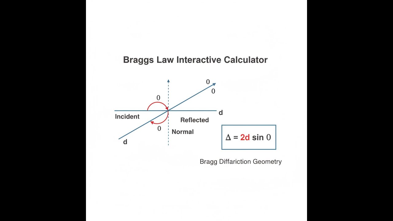
Bragg Diffraction Diagram

How to Use This Calculator
- Select your calculation mode from the dropdown — choose whether you want to solve for wavelength, lattice spacing, diffraction angle, order number, or maximum order.
- Enter the known values into the visible input fields: order (n), wavelength (λ) in Angstroms, lattice spacing (d) in Angstroms, and/or Bragg angle (θ) in degrees, as required by your selected mode.
- Check your inputs — order must be a positive integer, angle must be between 0° and 90°, and all physical quantities must be positive.
- Click Calculate to see your result.
Bragg's Law Calculator
Bragg's Law Interactive Visualizer
See how X-ray diffraction angles relate to crystal lattice spacing through the fundamental nλ = 2d sin θ relationship. Adjust parameters to understand constructive interference conditions in crystallography.
BRAGG ANGLE
14.5°
DETECTOR ANGLE
29.0°
PATH DIFF
1.54 Å
FIRGELLI Automations — Interactive Engineering Calculators
Bragg's Law Equations
Use the formula below to calculate diffraction conditions using Bragg's Law.
Fundamental Bragg Condition
nλ = 2d sin θ
where:
- n = order of diffraction (positive integer: 1, 2, 3...)
- λ = wavelength of incident radiation (Angstroms, Å)
- d = interplanar spacing (lattice spacing between parallel planes, Å)
- θ = Bragg angle (angle between incident beam and crystal planes, degrees or radians)
Derived Relations
Wavelength Calculation:
λ = (2d sin θ) / n
Lattice Spacing Calculation:
d = nλ / (2 sin θ)
Bragg Angle Calculation:
θ = arcsin(nλ / 2d)
Maximum Order Condition:
nmax = floor(2d / λ)
Since sin θ ≤ 1, the maximum order is limited by the ratio of lattice spacing to wavelength
Detector Angle (Scattering Angle)
2θ = 2 × θBragg
The detector angle (2θ) is the total scattering angle measured in X-ray diffraction experiments, equal to twice the Bragg angle. This is the angle between the incident beam direction and the scattered beam direction.
Simple Example
Given: n = 1, λ = 1.54 Å (Cu Kα), d = 2.82 Å
Calculate θ: sin θ = (1 × 1.54) / (2 × 2.82) = 0.2730, so θ = arcsin(0.2730) = 15.84°
Detector reads: 2θ = 31.68°
Result: The diffraction peak appears at a detector angle of 31.68°.
Theory & Practical Applications
Physical Basis of Bragg Diffraction
Bragg's Law describes the constructive interference condition that occurs when electromagnetic radiation (typically X-rays, but also electrons or neutrons) scatters from parallel planes of atoms within a crystalline material. The phenomenon was discovered by William Henry Bragg and his son William Lawrence Bragg in 1913, work that earned them the Nobel Prize in Physics in 1915. Unlike simple derivations that treat the crystal as a stack of perfect mirrors, the complete picture involves coherent scattering from all atoms in the crystal lattice, with the Bragg condition emerging as the specific geometric relationship where scattered waves from successive planes reinforce rather than cancel.
The critical insight is that incident radiation penetrates into the crystal and reflects from multiple parallel planes simultaneously. For constructive interference to occur, the path difference between rays reflecting from adjacent planes must equal an integer multiple of the wavelength. This path difference equals 2d sin θ, where d is the perpendicular distance between planes and θ is the angle of incidence measured from the plane surface (not from the normal, which differs from many optical conventions). When nλ = 2d sin θ, all reflected waves are in phase and produce a strong diffracted beam; at other angles, destructive interference eliminates the signal.
Lattice Planes and Miller Indices
The lattice spacing d in Bragg's Law refers to the perpendicular distance between specific crystallographic planes, identified by Miller indices (hkl). In a cubic crystal system with lattice parameter a, the d-spacing for planes (hkl) is dhkl = a/√(h² + k² + l²). For example, silicon has a = 5.431 Å; the (111) planes have d₁₁₁ = 5.431/√3 = 3.136 Å, while (220) planes have d₂₂₀ = 5.431/√8 = 1.920 Å. The same physical crystal contains infinite sets of parallel planes with different spacings, each producing diffraction at different angles. High-index planes (large h, k, l values) have smaller d-spacings and diffract at higher angles.
In non-cubic systems (tetragonal, hexagonal, orthorhombic, etc.), the relationship between Miller indices and d-spacing becomes more complex, incorporating multiple lattice parameters and angular relationships. Hexagonal systems require four-index notation (hkil) and separate a and c parameters. This geometric complexity is why X-ray crystallography software packages are essential for analyzing real materials—hand calculation is practical only for high-symmetry cubic systems.
Order Number and Higher-Order Reflections
The order number n represents constructive interference occurring when the path difference equals exactly n wavelengths. First-order diffraction (n=1) occurs at the lowest angle for a given d-spacing. Second-order diffraction (n=2) from planes with spacing d occurs at the same angle as first-order diffraction from planes with spacing d/2. This mathematical equivalence means that a second-order reflection from (111) planes is indistinguishable from a first-order reflection from (222) planes—they produce the same diffraction peak. In practice, crystallographers typically work with first-order reflections and reindex higher orders accordingly.
The maximum observable order is limited by the condition sin θ ≤ 1, which gives nmax = floor(2d/λ). For Cu Kα radiation (λ = 1.5406 Å) and silicon (111) planes (d = 3.136 Å), the maximum order is nmax = floor(2 × 3.136 / 1.5406) = floor(4.07) = 4. However, higher orders are progressively weaker due to the atomic form factor, which describes how scattering efficiency decreases with increasing angle. In materials with systematic absences due to the crystal's space group symmetry, certain orders may be forbidden entirely—for example, face-centered cubic (FCC) structures show reflections only when h, k, l are all even or all odd.
Wavelength Selection and Radiation Sources
Laboratory X-ray diffractometers typically use characteristic radiation from copper (Cu Kα, λ = 1.5406 Å), molybdenum (Mo Kα, λ = 0.7107 Å), or chromium (Cr Kα, λ = 2.2909 Å) targets. The choice affects the accessible range of d-spacings and angular resolution. Shorter wavelengths (Mo Kα) allow higher-order reflections and access to smaller d-spacings, important for complex structures, but produce peaks at lower angles where angular resolution is poorer. Copper radiation provides an excellent balance for most materials, with sufficient penetration depth and favorable peak positioning.
Synchrotron radiation sources produce tunable monochromatic X-rays with wavelengths typically from 0.4 to 2.5 Å, offering flexibility unavailable in laboratory sources. The very high intensity enables time-resolved studies (millisecond time scales), micro-beam analysis (sub-micron spatial resolution), and studies of weakly scattering samples. Neutron diffraction, using thermal neutrons with λ ≈ 1-2 Å, follows the same Bragg law but probes nuclear positions rather than electron density, providing complementary structural information particularly valuable for locating light atoms (hydrogen, lithium) in the presence of heavy elements.
Angular Resolution and Experimental Geometry
The Bragg angle θ is measured between the incident beam and the crystal planes, but diffractometers measure the detector angle 2θ, which is the total scattering angle. This factor of two is critical in experimental practice: if you calculate θ = 15.76° from Bragg's Law, you position your detector at 2θ = 31.52°. Confusion between θ and 2θ is a common source of error in crystallography. The Bragg-Brentano geometry, used in most powder diffractometers, maintains the θ-2θ relationship automatically through coupled goniometer motion, ensuring that the focusing condition is satisfied across the entire angular range.
Peak width in a diffraction pattern contains information beyond just the Bragg condition. The Scherrer equation relates peak broadening to crystallite size: τ = Kλ/(β cos θ), where τ is the mean crystallite dimension, K ≈ 0.9 is a shape factor, and β is the peak width in radians. This allows particle size determination in the nanometer range. Strain broadening adds another contribution, distinguishable from size broadening by its different angular dependence. Modern Rietveld refinement methods simultaneously fit all peaks in a powder pattern, extracting lattice parameters, atomic positions, thermal motion, crystallite size, and strain—far more information than the simple Bragg condition alone provides.
Industrial Applications Across Sectors
In the semiconductor industry, X-ray diffraction using Bragg's Law verifies epitaxial layer thickness and composition in devices like high-electron-mobility transistors (HEMTs) and laser diodes. For a GaN layer grown on sapphire, the (0002) reflection appears at 2θ ≈ 34.56° for Cu Kα radiation (d₀₀₀₂ = 2.593 Å). Strain in the layer shifts this peak; compressive strain increases 2θ, tensile strain decreases it. Peak splitting indicates composition gradients. Reciprocal space mapping extends this analysis to two dimensions, revealing misfit dislocations and relaxation processes critical for device reliability. Wafer curvature measurements combined with XRD provide complete stress tensors in multilayer stacks.
Pharmaceutical companies use powder X-ray diffraction (PXRD) for polymorph identification and quality control. Active pharmaceutical ingredients (APIs) often crystallize in multiple forms with different dissolution rates and bioavailability. Atorvastatin calcium, for example, exists in more than 70 crystalline forms. Each polymorph produces a unique "fingerprint" diffraction pattern determined by its crystal structure. Regulatory agencies require polymorph characterization in drug submissions, and production lines use real-time XRD monitoring to detect polymorph transitions during processing. The technique is non-destructive, requires minimal sample preparation, and provides quantitative phase composition in mixtures through Rietveld refinement or reference intensity ratio methods.
Materials research relies on Bragg diffraction for texture analysis (preferred crystallographic orientation) in rolled metals, extruded polymers, and thin films. Texture affects mechanical properties, magnetic behavior, and electrical conductivity. Pole figures, constructed by measuring reflection intensities at many sample orientations, quantify orientation distributions. In steel manufacturing, {100}<011> rolling texture improves deep drawability for automotive body panels, while {110}<001> cube texture is desired for electrical steels to minimize magnetic losses. Texture evolution during processing—cold work, annealing, recrystallization—is tracked via in-situ XRD with controlled temperature and stress environments, revealing fundamental deformation and recovery mechanisms.
Fully Worked Example: Silicon Wafer Characterization
Problem: A silicon wafer is analyzed using Cu Kα radiation (λ = 1.5406 Å) in a Bragg-Brentano diffractometer. The primary diffraction peak appears at detector angle 2θ = 69.13°. Determine: (a) the d-spacing of the diffracting planes, (b) the Miller indices if silicon has a diamond cubic structure with a = 5.4310 Å, (c) the Bragg angle θ and confirm the measurement geometry, (d) whether second-order diffraction is possible for these planes, and (e) the angular position where second-order diffraction would appear.
Solution Part (a) – Calculate d-spacing:
First, extract the Bragg angle from the detector reading: θ = (2θ)/2 = 69.13°/2 = 34.565°
Convert to radians for calculation: θ = 34.565° × (π/180°) = 0.6032 radians
For first-order diffraction (n = 1), rearrange Bragg's Law: d = nλ/(2 sin θ)
Calculate: d = (1 × 1.5406 Å)/(2 × sin(34.565°)) = 1.5406/(2 × 0.5671) = 1.5406/1.1342 = 1.3580 Å
Solution Part (b) – Identify Miller indices:
For cubic crystals: dhkl = a/√(h² + k² + l²), therefore: √(h² + k² + l²) = a/d
Calculate: √(h² + k² + l²) = 5.4310 Å / 1.3580 Å = 3.999 ≈ 4.00
Since √(h² + k² + l²) = 4, we need h² + k² + l² = 16
Possible combinations: (400), (040), (004) are equivalent by symmetry; or (220) gives 4 + 4 + 0 = 8, not 16
Checking (311): 9 + 1 + 1 = 11 (no); (222): 4 + 4 + 4 = 12 (no); (004): 0 + 0 + 16 = 16 (yes)
However, silicon has a diamond cubic structure (space group Fd-3m) with systematic absences. The (004) reflection is allowed. Given the near-perfect match at √16 = 4, the diffracting planes are (400) or equivalent (040), (004). By convention, we write the lowest index set: (400) planes.
Solution Part (c) – Verify geometry:
Bragg angle θ = 34.565° (calculated above from 2θ/2)
The Bragg condition states the angle is measured between the incident beam and the crystal planes
The detector measures total scattering angle = incident angle + exit angle = θ + θ = 2θ
Verification: 2 × 34.565° = 69.13° ✓ (matches measured detector position)
Solution Part (d) – Check second-order diffraction:
For second order (n = 2): sin θ₂ = (2 × 1.5406 Å)/(2 × 1.3580 Å) = 3.0812/2.7160 = 1.1345
Since sin θ₂ > 1, second-order diffraction is not possible for these planes with this wavelength
Physical interpretation: The wavelength is too long relative to the d-spacing. The maximum order is nmax = floor(2d/λ) = floor(2 × 1.3580/1.5406) = floor(1.764) = 1
Solution Part (e) – Second-order from other planes:
Although n = 2 is impossible for (400) planes, we can observe which other planes might show n = 2 reflections
Second-order from planes with d = 1.3580 Å is equivalent to first-order from planes with d = 1.3580/2 = 0.6790 Å
Calculate: √(h² + k² + l²) = 5.4310/0.6790 = 7.998 ≈ 8.00, so h² + k² + l² = 64
This corresponds to (800) planes, but checking silicon's structure factor: (800) is systematically absent in diamond cubic
Conclusion: No second-order reflection will appear at a position equivalent to (400) doubling
Key Insights: This problem illustrates that not all mathematical solutions correspond to physically observable reflections. The systematic absences due to diamond cubic symmetry eliminate many reflections that would be allowed in a primitive cubic structure. Additionally, the limitation imposed by sin θ ≤ 1 restricts observable orders—a fundamental constraint often overlooked in simple treatments. Real crystallographic analysis must account for space group symmetry, not just lattice geometry. The high angle of the (400) reflection (2θ = 69.13°) places it in a region where instrumental resolution is excellent but intensity is reduced due to the atomic form factor fall-off, requiring careful background subtraction and possibly longer counting times for accurate intensity measurement.
Advanced Topics and Limitations
Bragg's Law assumes perfectly elastic scattering (no energy loss) and parallel incident radiation. Real experiments involve beam divergence, sample imperfections, and instrument aberrations. The Darwin width describes the intrinsic angular range over which a perfect crystal diffracts, typically ~0.001° for Si(400) with Cu Kα. Mosaic crystals, composed of slightly misoriented blocks, have broader diffraction profiles called the mosaic spread, typically 0.01-0.1°. This broadening is beneficial for neutron monochromators, where reflectivity integrated over the mosaic distribution exceeds that of perfect crystals.
Dynamic diffraction theory, required for perfect crystals and thick specimens, treats the wavefield inside the crystal as a coupled system of forward and diffracted beams. Multiple scattering events cause intensity oscillations (Pendellösung fringes) and create total reflection conditions not predicted by kinematic (Bragg) theory. Simulation software like XOP or SHADOW traces beam propagation through crystals, essential for designing synchrotron beamlines where crystal monochromators must deliver specific bandwidths and focal properties. The transition from kinematic to dynamic regimes depends on crystal perfection and thickness—typically dynamic theory is required when sample thickness exceeds the extinction distance (micrometers for strong reflections, millimeters for weak ones).
Frequently Asked Questions
Free Engineering Calculators
Explore our complete library of free engineering and physics calculators.
Browse All Calculators →🔗 Explore More Free Engineering Calculators
About the Author
Robbie Dickson — Chief Engineer & Founder, FIRGELLI Automations
Robbie Dickson brings over two decades of engineering expertise to FIRGELLI Automations. With a distinguished career at Rolls-Royce, BMW, and Ford, he has deep expertise in mechanical systems, actuator technology, and precision engineering.
Need to implement these calculations?
Explore the precision-engineered motion control solutions used by top engineers.


